
Modern data centers are pushing optical interconnects to their limits. As training clusters scale from thousands to tens of thousands of GPUs, bandwidth demands are increasing at an unprecedented rate. Next-generation AI workloads rely on multi-terabit-per-second communication between nodes, driving a rapid shift toward high-density, low-power optical I/O built on silicon photonics.
Silicon photonics has emerged as a strong approach for high-volume manufacturing and energy-efficient optical integration. However, one long-standing bottleneck continues to constrain the scalability of photonic systems: the seamless integration of laser sources. Conventional approaches, including external laser coupling or co-packaged light engines, suffer from cost, alignment, reliability, and footprint challenges—especially as hyperscale environments require increasingly dense wavelength-division multiplexing (DWDM) architectures to multiply available bandwidth.
SCINTIL Photonics: Engineering Dense Multi-Wavelength Lasers for Silicon Photonics
SCINTIL Photonics is addressing this challenge with a heterogeneous integration platform designed to embed III-V laser functionality directly onto a silicon photonics wafer. Their proprietary SCINTIL Heterogeneous Integration Photonics (SHIP™) process enables dense multi-wavelength laser generation by bonding III-V dies at the wafer level after the silicon stack is flipped and waveguides are exposed via a handle exchange. The resulting single-chip, DWDM-native light engine, LEAF Light™, is implemented as a Photonic System-on-Chip (PSoC) built on SHIP™. LEAF Light™ enables low-power, high-density optical connectivity, delivering 6.4 Tbps/mm edge bandwidth density today, while significantly reducing power versus conventional pluggable solutions.
.png?width=929&height=271&name=Untitled%20design%20(9).png)
This unique approach delivers several key advantages for large-scale photonic integration:
-
-
-
Fully encapsulated lasers help protect against moisture and oxygen exposure, improving long-term reliability in data center environments.
-
Adiabatic transitions to the photonic integrated circuit (PIC) reduce dependence on anti-reflection coatings or high-precision optical alignment, improving yield and manufacturability.
-
A wafer-level bonding process aligns well with silicon photonics fabrication and supports high-volume production needs for AI-driven applications.
-
-
By targeting dense multi-wavelength laser sources tuned for DWDM architectures, SCINTIL Photonics is positioning its platform at the heart of AI data center connectivity.
Engineering a Custom Platform: Overcoming Design and PDK Development Barriers
Building a heterogeneous integration platform of this complexity requires more than just a bonding process — it demands a finely tuned ecosystem of photonic components that perform reliably under multi-wavelength laser operation. Since no existing process design kit (PDK) could support SCINTIL Photonics’ novel handle-exchange and III-V bonding flow, the team developed a fully custom PDK in-house.
Two key engineering challenges emerged during early development cycles:
-
-
-
Component-level optimization — Elements such as tapers, couplers, and bends had to be designed for minimal insertion loss and reduced back-reflections to ensure compatibility with integrated multi-wavelength lasers.
-
Robustness across process corners — Large, wavelength-dependent structures had to maintain predictable behavior across fabrication variability and thermal conditions common in data center environments.
-
-
With multiple photonic structures requiring iterative refinement under varying materials, geometries, and thermal conditions, rapid simulation was essential to reducing design risk and accelerating PDK maturity.
Accelerating Iteration with Flexcompute’s High-Performance Simulation Environment
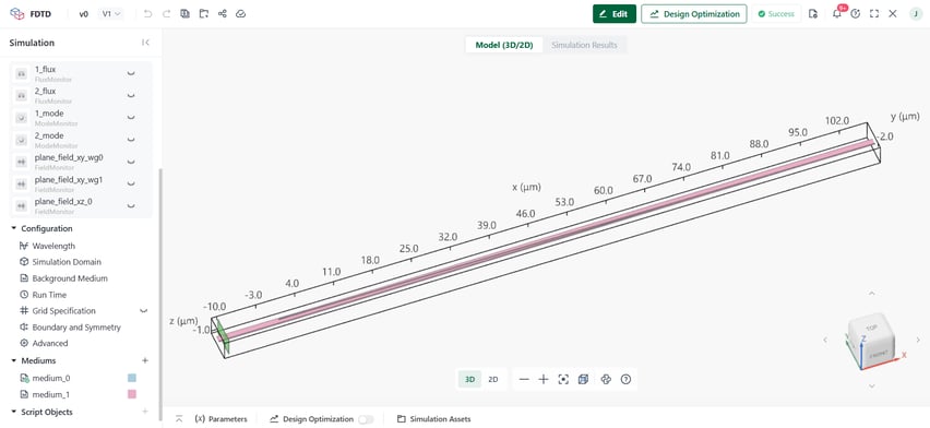
To meet the speed and precision requirements of their iterative design cycles, SCINTIL Photonics turned to Flexcompute’s high-performance simulation tools. Using Flexcompute Tidy3D, the engineering team was able to evaluate component designs quickly, experiment with different configurations, and resolve back-reflection and coupling efficiency issues early in development.
Several aspects of Flexcompute’s environment were especially valuable:
-
-
-
Fast turnaround time made it possible to test multiple design variations in parallel without slowing development progress.
-
Adjoint-based optimization via a Python-native API enabled automated refinement of geometries to improve performance without writing custom optimization infrastructure.
-
Ready-to-use examples and scripts helped the SCINTIL Photonics team quickly apply Tidy3D to their specific structures.
-
-
This helped SCINTIL Photonics iterate more frequently, evaluate design trade-offs with greater confidence, and streamline the path toward a manufacturable platform.
“We're using Tidy3D to optimize large passive devices on our proprietary photonics platform, and it's transformed how we work. What used to take days of waiting for simulation results now happens while I'm still analyzing the previous batch. We're making design decisions faster, backed by solid simulation data rather than educated guesses. The native Python API makes it easy for me to customize optimization trials to my needs, and I love being able to draw on the entire scientific Python ecosystem for additional functionality. The speed has let us explore design spaces faster, and I can spin up as many parallel runs as needed to comb the design space. I've been pleasantly surprised by the performance of the designs I've been able to find with the help of Tidy3D.”
- Jason Mak, Photonics Design Engineer
Scaling Toward Next-Generation Optical Interconnect Engines
Looking ahead, SCINTIL Photonics plans to continue advancing its dense multi-wavelength laser platform with a focus on increasing channel count, improving thermal stability, and reducing cost per optical port. As the industry progresses toward co-packaged optics and advanced photonic engines for AI infrastructure, scalable laser integration will remain a key differentiator.
With high-speed simulation workflows now integrated into their development process, SCINTIL Photonics is positioned to iterate faster and refine their platform as they move toward commercialization milestones.
Shaping the Future of AI Photonics Through Co-Design and Simulation
SCINTIL Photonics is tackling one of the final integration challenges in silicon photonics by enabling dense, multi-wavelength lasers designed for high-performance computing and AI infrastructure. Flexcompute’s simulation platform has helped compress design timelines and increase iteration velocity, reinforcing a development process that is both innovative and scalable.
As AI data centers continue to demand higher bandwidth, lower power, and greater integration density, partnerships between photonic platform developers and advanced simulation providers will play a defining role in shaping the next generation of optical connectivity.
.png)
-1.gif)
-1.gif)