
In this case study, we demonstrate loading a foundry PDK, performing RF and optical simulations, conducting time-domain analyses, and generating fabrication-ready layouts — all within a single interface. The example features an ultra-high-speed electro-optic modulator in thin-film lithium niobate (TFLN).
Background
Electro-optic Mach-Zehnder modulators (EO-MZMs) are essential in photonic integrated circuits (PICs), particularly for high-speed optical communication. These devices modulate light by changing the refractive index of a waveguide in response to an applied electric field—a process that requires careful coordination of electrical and optical properties.
Designing such devices traditionally involves fragmented workflows: separate tools for layout, electrostatic modeling, optical simulation, and data analysis. These disconnected steps can lead to inefficiencies, longer development cycles, and integration errors.
Explore the complete example: Electro-Optic MZM Example in PhotonForge Documentation
Challenges
To design and optimize EO-MZMs, engineers need to:
-
Accurately simulate the electro-optic effect, including voltage-induced refractive index changes.
-
Understand the interaction between RF electrodes and optical waveguides.
-
Quantify performance metrics like extinction ratio, insertion loss, and phase modulation efficiency.
-
Iterate rapidly on device geometry, electrode configuration, and material stack-up—all while ensuring fabrication readiness.
Traditional limitations:
-
Separate solvers for electrical and optical domains make co-simulation cumbersome.
-
Manual data exchange between tools increases the chance of error.
-
High computational costs due to 3D field simulations.
-
Limited layout-driven simulation capabilities inhibit rapid prototyping.
Solution with PhotonForge
PhotonForge unifies layout, electrostatic, and full-wave optical simulation within one cohesive platform. Using the Tidy3D engine, PhotonForge allows for:
-
Electro-optic co-simulation using voltage-dependent permittivity mapping
-
GPU-accelerated FDTD simulation for rapid optical modeling
-
Scriptable Python interface for parameter sweeps and design automation
-
Drag-and-drop layout tools for fast, fabrication-aligned design creation
-
Direct GDS import/export for seamless foundry integration
-
3D field visualization of electric and optical field distributions
Design details
The EO-MZM design in this case study includes:
-
Y-splitter: An input waveguide splits the optical signal into two arms.

-
Phase modulator arms: Each arm contains a straight waveguide surrounded by metal electrodes. A voltage applied to these electrodes induces an electric field that modifies the local refractive index.

-
Whole device: Integrate the edge couplers with the MZM and create a complete device.

Simulation process
-
Layout construction:
The entire modulator geometry, including optical waveguides, cladding layers, and electrode geometries, is created in PhotonForge using its layout editor or scriptable Python interface.
-
RF photonic solver:
PhotonForge calculates the electric field distribution generated by the applied voltage. From this field, the change in refractive index is computed using the linear electro-optic (Pockels) effect for the selected material (e.g., LiNbO₃, silicon, etc.).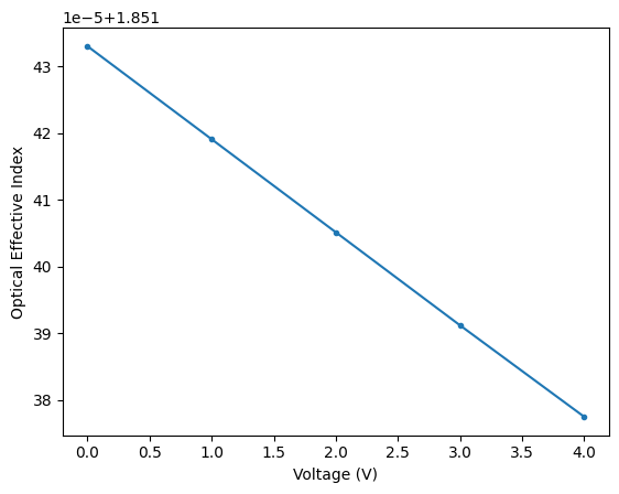
-
Permittivity mapping:
The induced index change is transformed into a spatially varying permittivity map, which is then used to perturb the optical domain for accurate co-simulation.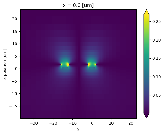
-
FDTD Simulation:
The perturbed structure is simulated using Tidy3D’s GPU-accelerated FDTD solver to analyze how the modulated index distribution affects light propagation.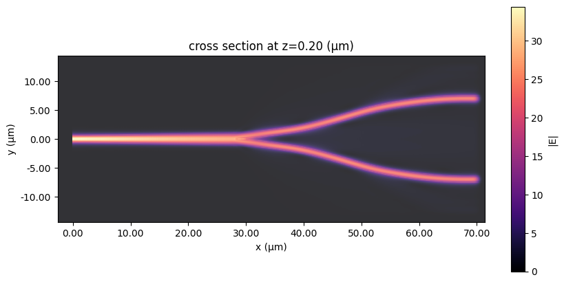
-
Result analysis:
The output fields are analyzed to determine: insertion loss, extinction ratio (ER), phase shift efficiency, and output intensity modulation vs. input voltage.
Results
Using PhotonForge, the simulated EO-MZM achieved:
-
High extinction ratio: ~20–30 dB depending on phase mismatch
-
Insertion loss: Maintained below 1 dB with optimized tapers
-
π-phase shift voltage-length product (VπL): Tunable via electrode spacing and material selection
A full 3D model's complete co-simulation runtime is under 10 minutes. The in-built visualization tools provide 3D overlays of both the optical and electric fields, enabling intuitive debugging and optimization. Cross-sectional slices and field animations provide insights into wave interference dynamics and loss mechanisms.
Advantages Over Traditional Tools
| Feature | Traditional Workflow | PhotonForge |
|---|---|---|
| Electro-optic co-simulation | Manual, disconnected tools | Fully integrated |
| Layout-to-simulation | Manual translation | Automated, layout-driven |
| GPU acceleration | Often CPU-bound | Native GPU support |
| Design automation | Limited | Python scripting |
| 3D visualization | Basic or missing | Advanced GUI with overlays |
| Foundry-ready PDK support | Often custom-built | Built-in and customizable |
Conclusion
This case study illustrates how PhotonForge transforms the workflow for designing and simulating electro-optic modulators. With a unified environment that supports full electro-optic co-simulation, high-performance GPU-based FDTD solvers, and fabrication-ready layouts, engineers can now:
-
Rapidly iterate on device concepts
-
Confidently evaluate performance
-
Streamline handoff to fabrication
Whether you're developing cutting-edge optical interconnects or optimizing modulators for quantum applications, PhotonForge allows you to move faster, with accuracy and confidence.
Explore the example
Electro-Optic MZM Example in PhotonForge Documentation
.png)