Finite-difference time-domain (FDTD) simulation is the gold standard for modeling photonic devices. It solves Maxwell’s equations directly in space and time, making very few assumptions. That generality makes FDTD an excellent reference method but it also means that its computational cost grows with the physical volume of the device.
Eigenmode expansion (EME) offers a compelling alternative for structures that evolve primarily along a well-defined propagation direction. EME represents the electromagnetic field as a superposition of local cross-sectional eigenmodes. It then propagates those modes through a sequence of cells and accounts for coupling at the interfaces between them. Because the longitudinal direction is treated analytically within each cell, EME can model long components very efficiently.
EME is commonly used to simulate long tapers, multimode interferometers (MMIs), and directional couplers. However, it is less widely known that EME is equally useful for waveguide bends, including bends made from anisotropic materials. Here, we benchmark Tidy3D’s EME solver against full 3D FDTD for a 90° Euler bend on an X-cut thin-film lithium niobate (TFLN) platform.
How EME models a bend
In an EME simulation, the device is divided into cells along a longitudinal propagation coordinate. Within each cell, the field is expanded in the local eigenmodes:

The modal amplitudes are transferred between adjacent cells by overlap matrices. A bend uses the same principle in a curvilinear coordinate system: the mode planes rotate along the waveguide centerline, and the solver propagates the modal basis through this sequence of orientations.
This point is especially important for anisotropic materials. In X-cut lithium niobate, the optical axis lies in the plane of the chip. We orient that axis along the global yyy direction. As the bend turns through 90°, its local propagation and transverse axes rotate relative to the fixed lithium-niobate crystal axes. In the local coordinate frame, the permittivity tensor therefore becomes
.png?width=308&height=28&name=lagrida_latex_editor%20(1).png)
and generally develops off-diagonal terms. The local quasi-TE and quasi-TM states evolve and can couple as the propagation direction changes.
Benchmark device
The simulated device is a symmetric 90° Euler bend with straight input and output sections. The modeled cross section is a thick-film, deeply etched TFLN rib waveguide: a 900 nm LN film is etched by 600 nm, leaving a 300 nm residual slab. The model also includes the sloped sidewalls that arise in lithium-niobate dry etching.
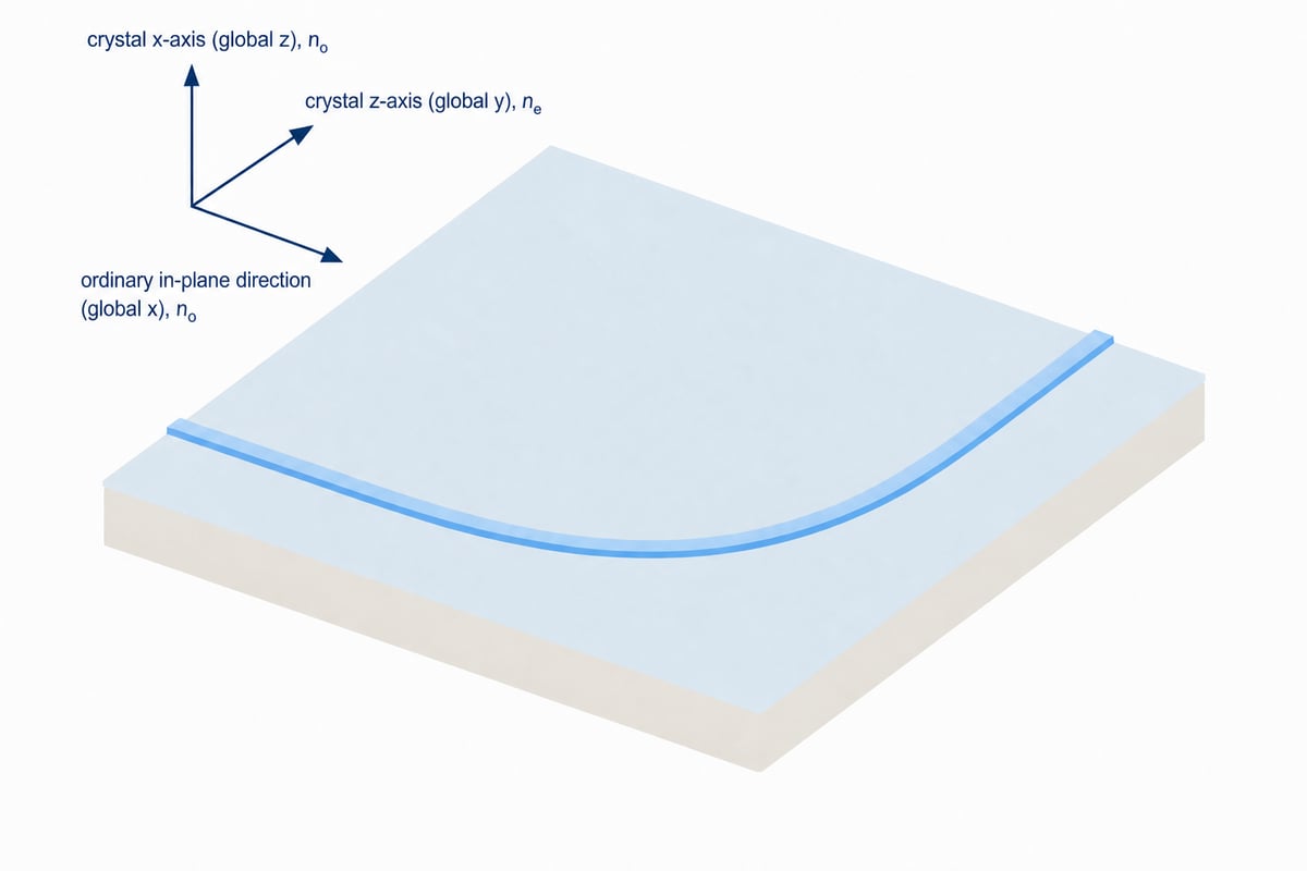
Figure 1. Schematic rendering of the 90° Euler bend.
The geometry is summarized below.
|
Parameter |
Value |
|---|---|
|
Crystal cut |
X-cut lithium niobate |
|
Optical-axis orientation |
Global yyy, in the bend plane |
|
LN film thickness |
900 nm |
|
Etch depth (ridge height above slab) |
600 nm |
|
Residual slab thickness |
300 nm |
|
Ridge top width |
900 nm |
|
Sidewall angle |
70° from horizontal |
|
Cladding/background |
SiO2 |
|
Broadband effective radius |
10 µm |
FDTD setup
The FDTD simulation uses a broadband fundamental quasi-TE mode source in the straight input waveguide and a mode monitor in the straight output waveguide. The output monitor performs modal decomposition so the reported transmission is the power in the outgoing fundamental quasi-TE mode normalized to the launched modal power.
The spatial grid is set to 40 steps per wavelength in the material-aware automatic nonuniform mesh.
EME setup
The EME model follows the approach in Tidy3D’s anisotropic-bend EME tutorial. Its propagation path is divided into three regions:
-
One uniform cell for the straight input section.
-
Ten curved cells whose individual bend radii follow the local curvature of the 90° Euler bend.
-
One uniform cell for the straight output section.
The Euler section is therefore not treated as a single-radius circular arc. At the center of each bend cell, the local curvature  is sampled and the cell is assigned the corresponding radius magnitude
 -1.png?width=116&height=21&name=lagrida_latex_editor%20(1)-1.png) . For the 10 µm effective-radius bend, these cell radii are approximately 100, 33.3, 20, 14.3, 11.1, 11.1, 14.3, 20, 33.3, and 100 µm.
. For the 10 µm effective-radius bend, these cell radii are approximately 100, 33.3, 20, 14.3, 11.1, 11.1, 14.3, 20, 33.3, and 100 µm.
At every mode plane, the solver computes and propagates 16 modes. Retaining more than only the desired guided mode is essential: radiation-like and higher-order basis states mediate the field redistribution between neighboring rotated cross sections. The mode-plane domain is 9 × 6 µm, and the transverse mesh uses the same wavelength/40 setting as FDTD.
For the anisotropic bend, bend_medium_frame="global" keeps the physical lithium-niobate crystal axes and the laboratory-frame permittivity tensor fixed as the waveguide rotates. When that fixed tensor is expressed in each rotating local mode-plane basis, its matrix components change and generally acquire off-diagonal terms. For the broadband sweep, mode tracking is anchored at the central frequency to maintain the identity of the target mode across wavelength.
To ensure accuracy, we performed convergence tests on the number of EME cells, the transverse mesh resolution, and the number of modes used in each cell.
Broadband FDTD–EME comparison

Figure 2. Fundamental quasi-TE transmission through the 10 µm effective-radius X-cut TFLN Euler bend. The vertical range is 0.5–1.0 to show the full target-channel response while keeping the FDTD–EME separation visible.
First, we used a bend with a 10 µm effective radius and simulated its broadband response. FDTD and EME give very consistent results: across 1520–1580 nm, the mean relative transmission difference is 0.430% and the maximum is 0.566%. The broadband FDTD run cost 15 FlexCredits, compared with 1.31 FlexCredits for EME, a reduction of approximately 11.4× for this case.
Transmission versus bend radius
When designing bends, one often wants to know the loss as a function of bend radius. Bend-radius sweeps are where the EME cost advantage becomes particularly clear. We simulated effective radii of 5, 7.5, 10, 15, and 20 µm at 1550 nm.
Fundamental-mode transmission versus effective bend radius

Figure 3. Fundamental quasi-TE transmission at 1550 nm versus effective radius. The FDTD curve is drawn above the EME curve so that both remain visible where they overlap.
Both methods reproduce the expected strong increase in target-mode transmission as the effective radius grows. The maximum absolute transmission difference is 0.0126. The relative difference is 4.61% for the aggressive 5 µm bend and no more than 1.49% from 7.5 to 20 µm, while the computational costs are drastically different.
Actual FlexCredit cost versus effective bend radius

Figure 4. Actual FlexCredit cost for each single-wavelength radius simulation. FDTD cost rises with the physical footprint, whereas EME cost remains essentially constant for the fixed cell and modal discretization.
The FDTD cost increases from 5.076 FlexCredits at 5 µm to 32.661 FlexCredits at 20 µm. The corresponding EME calculation costs 0.576 FlexCredits at every radius. With the number of cells, transverse mesh, and propagated modes fixed, the EME matrix size is nearly independent of radius. Increasing the radius changes the physical cell lengths and phase accumulation, but not the number of modal unknowns.
For the complete five-radius sweep, FDTD consumed 85.088 FlexCredits and EME consumed 2.882 FlexCredits in total. That is a 29.5× cost reduction. The advantage grows rapidly with radius: EME is about 8.8× cheaper at 5 µm and 56.7× cheaper at 20 µm.
Conclusion
EME is not a replacement for FDTD in every photonic problem. Devices with strong backscattering, resonant behavior, multiple simultaneous or branching propagation paths, or no clear propagation path are better suited to FDTD. For a smooth waveguide bend, however, EME captures the essential physics with far lower computational cost.
For this X-cut TFLN 90° Euler bend, the EME model agrees with FDTD with reasonable accuracy. When designing bends, especially large bends, it is recommended to start with EME and then use FDTD for final verification. The same principle applies to designing long tapers and MMIs.
Reproducibility
The clean scripts used to generate the results can be downloaded below: