THE PIC DESIGN LANDSCAPE HAS COMPLETELY CHANGED
Agentic AI now designs photonic components end-to-end. One loop drives very different problems, from a single passive device to a full system-level link. The same approach that took an engineer weeks now runs in hours.
AGENTIC PHOTONIC CHIP DESIGN
From device to system-level simulations, in one workflow
INTRODUCTION
For years, designing a photonic chip meant hopping across a dozen disconnected tools, hand-authoring every component, and waiting days for each simulation. The steps that mattered most, robustness, post-layout simulation, and yield, were too expensive to run, so teams skipped them and found the failures on silicon.
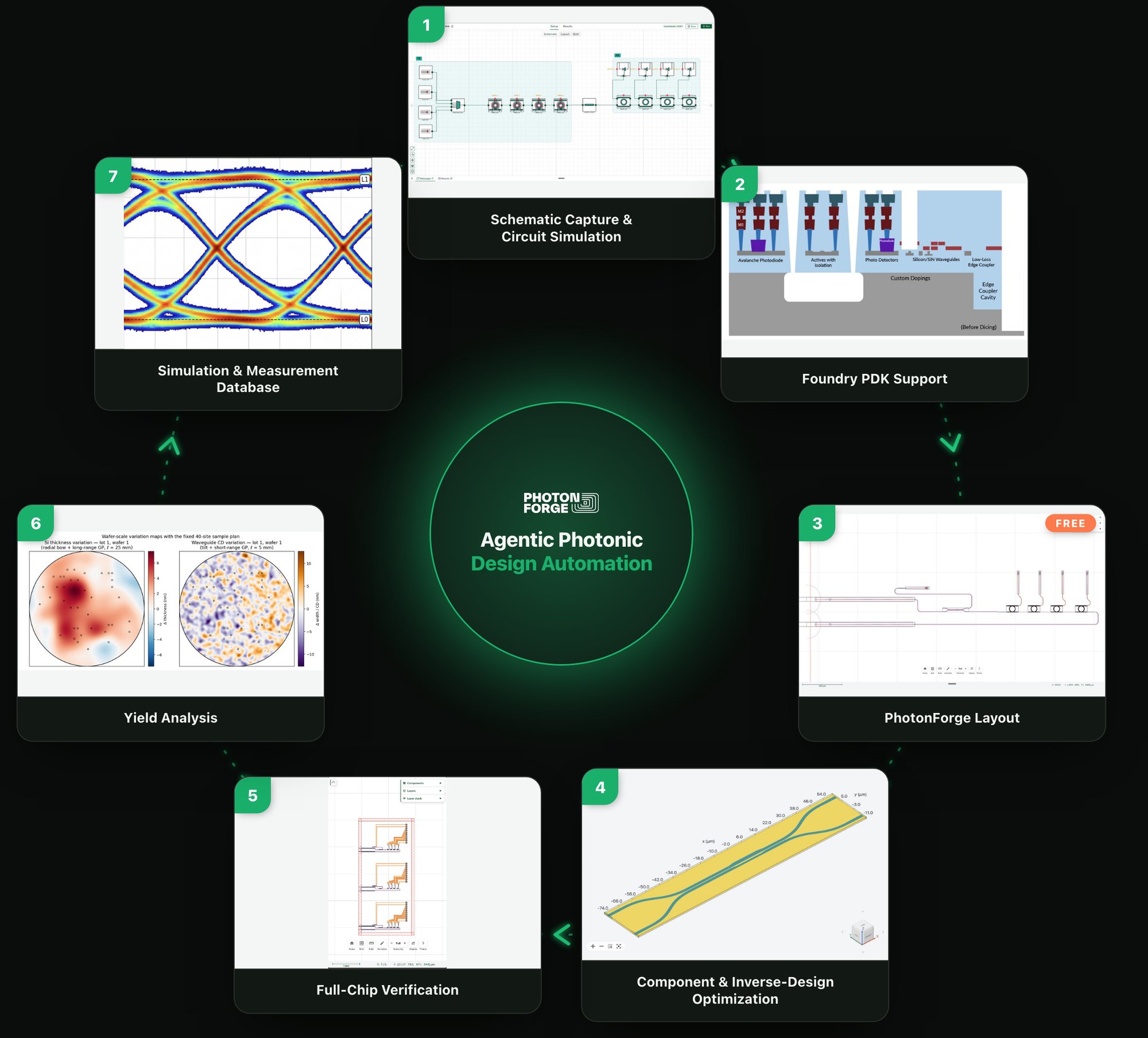
That has changed. With simulation that finishes in minutes and a workflow built to be AI-native, an agentic loop now runs the full design cycle: it reviews a design, forms a hypothesis, simulates, and keeps or discards on its own, across problems as different as a passive splitter and a full system-level link. The work that took an engineer weeks now runs in hours, and the steps that used to get skipped run automatically.
HOW AI AGENTS, PHOTONFORGE, AND TIDY3D ENABLES THIS
All of this runs on Flexcompute's photonics design suite, driven by AI.
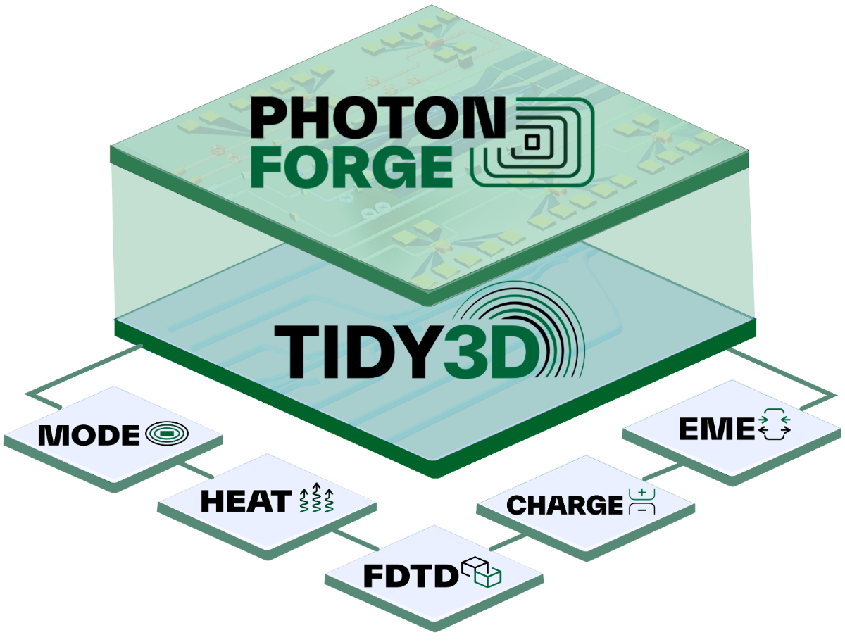
Tidy3D provides compute: GPU-native, multiphysics simulation, FDTD, mode, heat, and RF, with runs that finish in minutes rather than days. PhotonForge is the design environment on top, and every layer of it, from the GUI to Python, is built to be AI-native. You drive the same design and the same data three ways: point and click in the Photonic Canvas, write Python, or hand it to an AI agent that works headless.
Put together, AI agents plus PhotonForge plus Tidy3D let one agentic loop carry a design end-to-end. The solver automatically switches to match the physics, so the same loop that optimizes a passive device also closes a full system-level link and runs the verification and yield checks that the old flow was forced to skip.

WHAT PHOTONFORGE IS, AND THE PROBLEM IT SOLVES
So what is PhotonForge, and why did we build it?
Designing a chip for production spans many hands. One design crosses component designers, system designers, layout engineers, and measurement engineers, as well as the foundry and the EDA ecosystem, before it reaches silicon. Each hand-off is manual, a tape-out takes months and six figures, and one missed step costs a full cycle. That fragmentation is the real problem.
PhotonForge removes it. It is a unified, version-controlled, traceable, and collaborative canvas for designing photonic chips for production, one workflow spanning PIC design, simulation, and measurement. Not a layout tool bolted onto a circuit simulator, but a single environment where the whole team, and now AI agents, work on the same design.
WHAT WE WILL COVER
In this hands-on seminar, we take a photonic design from a single component to a manufacturable circuit, and show how to drive the whole workflow with AI. You will see:
-
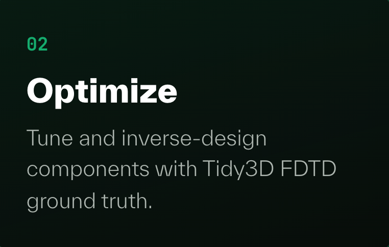
Component design and optimization, with the solver matched to the physics, up to inverse design
-
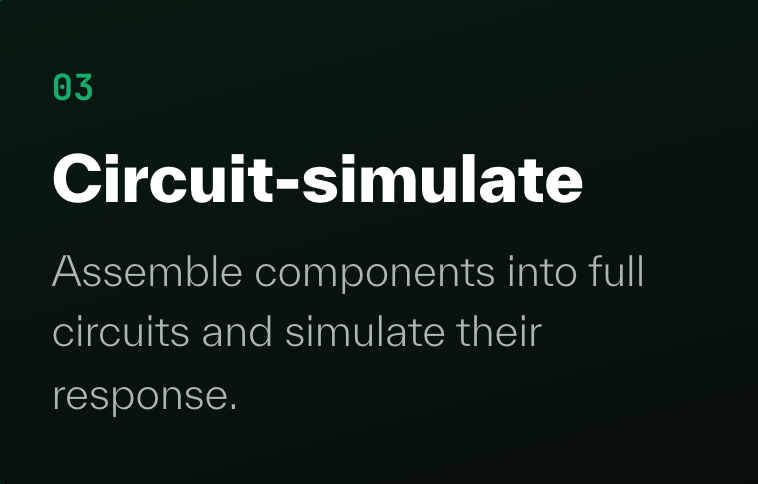
Circuit and system-level simulation, from device models to a full link
-
Working across Foundry PDKs and taking a design to a manufacturable layout
-
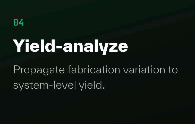
Verification and manufacturing with AI: DRC, layout inspection, and wafer-scale yield before tape-out
-
One agentic loop running the full cycle: review, hypothesize, simulate, keep or discard
-
Practical patterns for using AI tools well: what to hand the agent, how to keep an engineer in the loop, and how to verify what the AI produces

SPEAKERS
Prashanta Kharel, PhD
Bio: Prash earned his Ph.D. in Physics from Yale University, focusing on nonlinear optics and quantum photonics. He has authored over 20 publications and holds multiple patents. His work bridges photonic device research with scalable chip design and manufacturing. He is currently the Technology Strategist at Flexcompute, where he leads photonic design automation and industry collaborations.
Bohan Zhang, PhD
Bio: Bohan earned his Ph.D. in Electrical and Computer Engineering from Boston University. His work focuses on inverse design and automation for photonic integrated circuits. He has contributed to advanced design verification, optimization, and simulation tools for photonics, enabling faster and more reliable device development. Bohan is currently a Senior Research Scientist at Flexcompute, where he develops photonic design automation.
REWARDS FOR ATTENDING
-
Attending a seminar or hackathon gains 💰 50 FlexCredits
-
Submit a result in hackthon gains 💰 100 FlexCredits
-
Run your first simulation (get inspiration from PhotonForge example library) to earn 💰 50 FlexCredits
- For new users, install PhotonForge on either Python Client or the GUI to earn 💰 15 FlexCredits


.png?width=2000&height=727&name=photonforge%20tiers%20(1).png)