
PIC designers today jump between disconnected tools for schematic capture, simulation, layout, and verification, each with its own data model and file formats. Every handoff introduces translation risk, slows the path from concept to tape-out, and increases the chance of costly tape-out errors.
PhotonForge's Photonic Canvas is a unified design environment where schematic, simulation, layout, and verification operate on a single set of design data.
Capture Design Intent Your Way
In the GUI, designers load foundry PDKs and immediately see available components, with PCell parameter forms generated directly from the design data. They build circuits using PDK components, abstract components, and compact models, then run time-domain and frequency-domain circuit simulations without switching tools.
In Python, the same design data is fully accessible for scripting parametric designs, generating layouts, and automating simulation sweeps. Both the GUI and Python read and write the same underlying design with no translation step between them. A parameter changed in one is immediately reflected in the other. PCell forms in the GUI render directly from the component definition.
This flexibility extends to layout: schematic intent can drive automated layout generation, or designers can build layouts directly in Python.
One Design, Every View
In most PIC tool chains, the schematic, simulation setup, and layout are separate artifacts that must be kept in sync manually. In Photonic Canvas, they are views of the same design data.
This enables version control, design lifecycle management, and real-time team collaboration on a single set of design data.
GPU-Accelerated Simulation, Fully Integrated
Photonic Canvas interfaces directly with Flexcompute's Tidy3D multiphysics platform: FDTD and MODE solvers for optical simulation, CHARGE and HEAT for active device characterization, and RF analysis for high-speed modulators.
Component-level simulations generate compact models that feed directly into circuit-level analysis, taking designers from device characterization to full-system signal integrity (BER, eye diagrams) in a single workflow.
Fabrication-Aware Design
Foundry PDKs load natively, ensuring component placement and routing respect real-world process constraints. Internal LVS checks catch schematic-to-layout mismatches early, DRC integration with KLayout verifies designs against foundry rules, and a Cadence Virtuoso interface via Open Access connects to existing enterprise EDA flows.
Built for Real-World Complexity
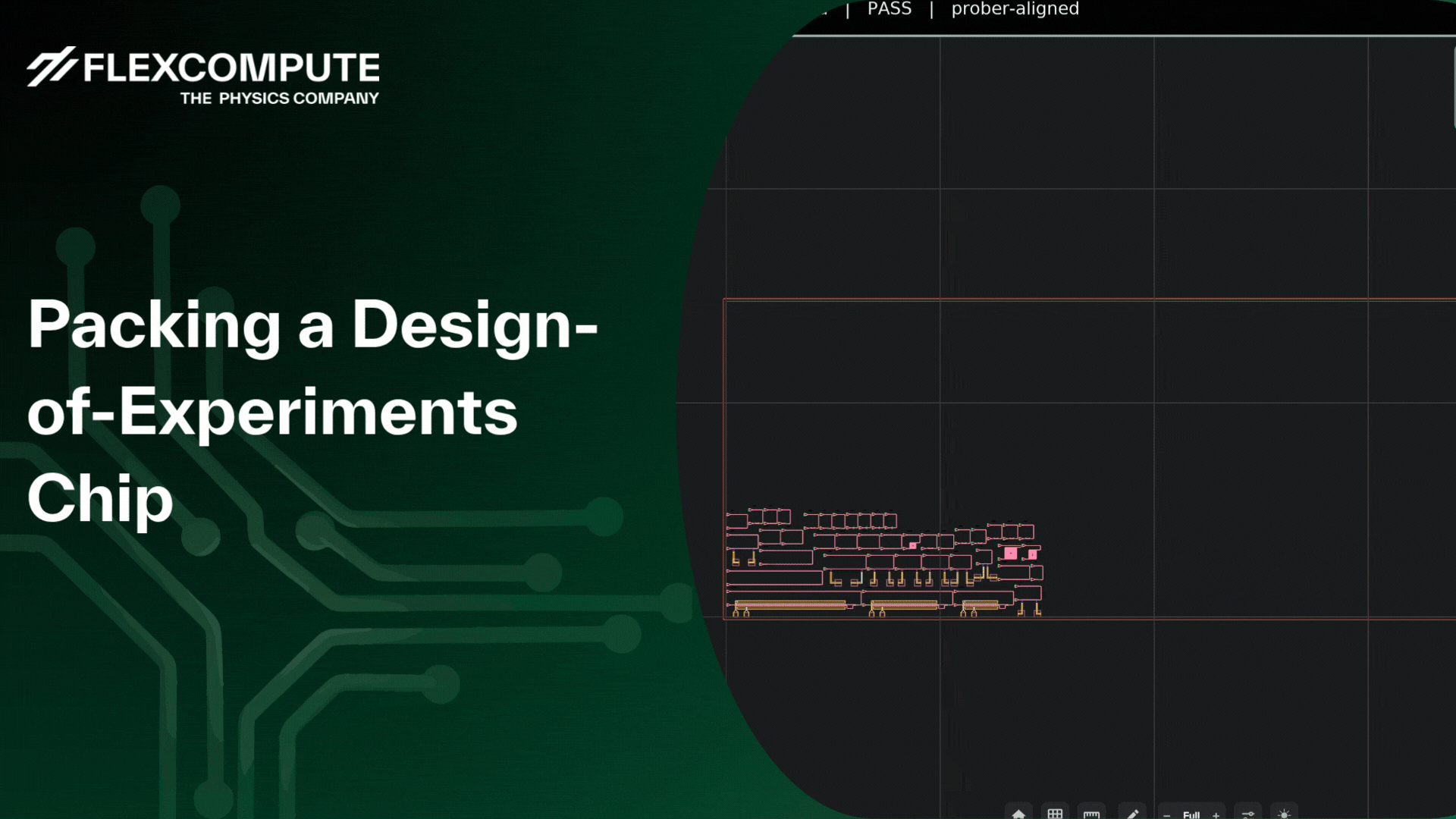
Complex photonic systems, including 3D-stacked electronic-photonic interposer dies, contain millions of layout elements. Photonic Canvas includes a high-performance 2D viewer, purpose-built for this scale, so designers can navigate full production layouts without performance degradation.
Ready for AI-Assisted Design
Because design data is structured, versioned, and fully accessible through Python, the environment is ready for AI-powered workflows. Agents can query designs, suggest optimizations, run simulation sweeps, and modify parameters through the same interface that human designers use. This is a direct consequence of how the platform is built today.
Why This Matters Now
The demand for photonic integration is accelerating with AI infrastructure and data center bandwidth requirements grow, while chip complexity is compounding. Photonic Canvas provides the unified, collaborative, fabrication-aware design environment the industry needs, built on GPU-accelerated simulation and architected for AI-assisted design.

-1.gif)
-1.gif)