PhotonForge is revolutionizing photonic integrated circuit (PIC) design by seamlessly integrating layout creation and circuit simulation into a unified platform. This integration streamlines the design process, enabling engineers to transition effortlessly from schematic layouts to comprehensive circuit simulations.
From Layout to Circuit Simulation
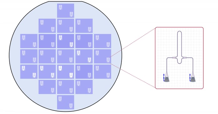
Traditionally, designing PICs involved multiple tools for layout and simulation, often leading to inefficiencies and potential errors during data translation. PhotonForge addresses this challenge by allowing users to import GDSII or OASIS layout files directly into the platform. Once imported, the software automatically detects components and their interconnections, constructing a corresponding circuit model ready for simulation.
This capability is exemplified in the PhotonForge example - Building Circuit Models from Layout Files, where a detailed guide walks users through building circuit models from layout files. The tutorial demonstrates how to:
-
Import layout files and assign ports.
-
Define models for each component.
-
Assemble the circuit by connecting components based on the layout.
By consolidating these steps within a single environment, PhotonForge eliminates the need for manual data transfer between disparate tools, reducing the risk of errors and accelerating the design cycle.
Advantages of Integrated Design and Simulation
1. Efficiency and Speed: With layout and simulation housed under one roof, engineers can iterate designs rapidly, testing various configurations without the overhead of exporting and importing data between separate applications.
2. Accuracy: Directly linking the physical layout to the simulation model ensures that analyses are based on the actual design, enhancing the reliability of simulation results.
3. Flexibility: PhotonForge supports various simulation types, including optical, thermal, and electrical analyses, allowing for comprehensive evaluation of PIC performance under different conditions.
4. Collaboration: The platform's unified environment facilitates better collaboration among design teams, as all members can access and work on the same project without compatibility issues.
Real-World Application
Consider a scenario where an engineer needs to assess the impact of thermal effects on a complex PIC layout. Using PhotonForge, they can:
-
Import the existing layout file.
-
Assign thermal models to relevant components.
-
Simulate the circuit to observe temperature distributions and identify potential hotspots.
-
Iterate the design to mitigate thermal issues, all within the same platform.
This integrated approach saves time and enhances the final design's quality by allowing for thorough, multi-physics analysis.
Conclusion
PhotonForge's capability to bridge the gap between layout design and circuit simulation marks a significant advancement in photonic design automation. By providing a cohesive environment for both tasks, it empowers engineers to develop more efficient, accurate, and reliable photonic integrated circuits.
For a hands-on demonstration and detailed guidance, refer to the PhotonForge tutorial on building circuit models from layout files and the simulation setup in the GUI.
-1.gif)
-1.gif)