In the rapidly evolving photonic integrated circuits (PICs) field, efficient and accurate design workflows are paramount. PhotonForge, Flexcompute’s next-generation photonic design automation platform, addresses this need by offering robust support for both foundry-provided and custom Process Design Kits (PDKs). This capability empowers engineers to create fabrication-ready designs tailored to specific manufacturing processes.
Understanding PDKs in Photonic Design
A Process Design Kit (PDK) is a comprehensive library of components, design rules, and simulation models provided by a semiconductor foundry. In photonics, PDKs include essential elements such as waveguides, modulators, and detectors, along with associated fabrication constraints like layer thicknesses and etching depths. Utilizing PDKs ensures that designs are compatible with the foundry's manufacturing capabilities, reducing the risk of costly errors during fabrication.
Custom PDK Creation with PhotonForge
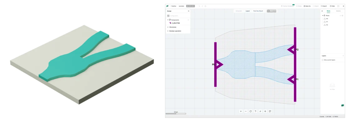
PhotonForge stands out by enabling users to leverage existing foundry PDKs and develop custom PDKs tailored to unique project requirements. See a PhotonForge example Y Splitter, and the simulation setup in the GUI. We find the key features:
-
Intuitive Layout Editor: Designers can create and modify photonic components using a user-friendly interface that supports graphical and script-based inputs.
-
Parameterized Cells (PCells): PhotonForge allows the creation of PCells, which are reusable, parameter-driven components that adapt to different design specifications.
-
Integration with Simulation Tools: Custom PDKs can be seamlessly integrated with Tidy3D's suite of simulation tools, including FDTD, MODE, RF, and CHARGE solvers, facilitating comprehensive design validation.
Advantages of Custom PDKs in PhotonForge
-
Design Flexibility: Custom PDKs allow for innovation beyond standard component libraries, enabling the development of novel photonic devices.
-
Process Compatibility: Tailoring PDKs to specific fabrication processes ensures that designs meet all manufacturing constraints, enhancing yield and performance.
-
Accelerated Development: By reusing and adapting PCells, designers can rapidly iterate on designs, reducing time-to-market.
-
Collaborative Workflows: PhotonForge's cloud-based environment supports collaborative development of PDKs, allowing teams to share and manage design resources efficiently.
In summary, Tidy3D's capability to create and manage custom PDKs provides photonic designers with the tools necessary to innovate and adapt in a fast-paced industry. By bridging the gap between design and fabrication, Tidy3D ensures that photonic devices are theoretically sound and practically manufacturable.
For a visual overview of PhotonForge's capabilities, you may find the video informative.
-1.gif)
-1.gif)